Проект УНТЦ P406
Краткое описание проекта
Название проекта:
Усовершенствование качества монокристалів (Cd,Zn)Te для целей детектирования гамма излучения при комнатной температуре
Руководитель проекта: Кутний, Владимир Евдокимович (к.т.н.), Национальный научный центр "Харьковський физико-технический институт", Харьков, Украина
Куратор проекта: Dr. Ralph James, Брукхэйвенская национальная лаборатория, Upton, NY, США
Организации-участники:
Национальный научный центр ХФТИ, Харьков, Украина, руководитель группы: Кутний, Владимир Евдокимович (к.т.н.)
Черновицкий национальный университет, Черновцы, Украина, руководитель группы: Проф. Фочук, Петр Михайлович, (д.х.н.)
Институт монокристаллов НАН Украины, Харьков, руководители: Космына, Мирон Богданович (д.т.н.), Коваленко, Назар Олегович (к.ф.-м.н.)
Финансирование: Министерство энергетики, США
Продолжительность: Два года, окончание февраль 2015 г.
Цель проекта
Основная цель проекта — улучшение качества монокристаллов (Cd,Zn)Te путем совершенствования технологий выращивания и послеростовой обработки
Описание работ
Применение тиглей с каналом для затравки при выращивании кристаллов твердого раствора CdZnTe позволило нам получать большие центральные монокристаллические блоки, которые наследуют ориентацию затравки. В таком кристалле размер монокристалличекого блока составлял до 40 % его размера. Разработанное ростовое оборудование и система управления им позволяют воспроизводимо получать слитки CdZnTe с высоким электрическим сопротивлением (~1010 Ом×см) и структурным совершенством (Рис. 1 и 2).
Высокотемпературная обработка кристаллов CdZnTe детекторного качества при избыточном давлении разных составляющих элементов продемонстрировала возможность резкого уменьшения размера и концентрации включений Te при избыточном давлении паров Cd, Zn или Te, или же в вакууме. Это, в свою очередь приводило к улучшению сбора заряда и энергетического разрешения детектора [5] (Рис. 3). Приходится считаться с тем, что отжиг – это сложная процедура, которая зависит не только от температуры, времени, и типа избыточного давления, но также и от структуры кристалла, природы его точечных дефектов, его дислокационной сетки и содержания легирующих примесей.
Мы промоделировали прохождение гамма-излучения через детектор, используя методику Монте-Карло в пакетах EGSnrc и Geant4 v4.9.6 для расчета транспорта фотонов и электронов [15]. Выбрав в качестве модельных параметров время формирования импульса, эквивалентный шумовой заряд и частоту выборки канала АЦП, мы получили амплитудные спектры и смогли их проанализировать и сравнить со спектрами, полученными экспериментально. То же было проведено для детекторов с контактом Шоттки [13] (Рис. 4). Важным параметром является отношение произведений подвижности и времен жизни, (μτ)e/(μτ)h. Мы показали, что CdZnTe детекторы сохраняют свои спектрометрические качества, когда отношение (μτ)e/(μτ)h менее 20. Эти критерии устанавливают требования к выращиванию CdZnTe кристаллов спектрометрического качества.
Было проанализировано влияние газостатической обработки при повышенной температуре на электрофизические свойства детекторов гамма-излучения структуры Au-CZT-Au. Измерения электрических и детектирующих свойств Au-CdZnTe-Au показали, что в процессе газстатической обработки происходит модификация контакта Au-CdZnTe, что, в свою очередь, ведет к увеличению электрического сопротивления и чувствительности к рентгеновскому и низкоэнергетическому гамма-излучению (Рис. 5).
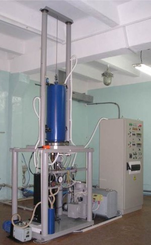 Рис. 1. Установка для роста кристаллов методом Бриджмена под высоким давлением инертного газа в Институте монокристаллов, Харьков. |
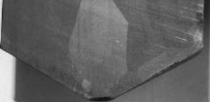 Рис. 2. Слиток CdZnTe, выращенный на затравке. |
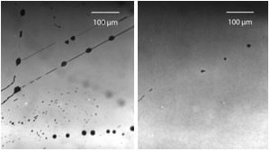 Рис. 3. Инфракраснасная микроскопия образца CdZnTe до (слева) и после (справа) отжига и закалки. |
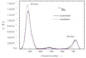 Рис. 4. Моделирование отклика детектора Ni/CdZnTe/Ni с барьером Шоттки на гамма-излучение от источника 133Ba после вычитания фонового шума. |
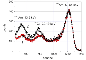 Рис. 5. Амплитудный спектр изотопов 137Cs и 241Am, полученный детекторомo структуры Au-CdZnTe-Au: 1. до газостатической обработки; 2. после обработки. |
Публикации
-
V. Tomashyk, P. Feychuk, L. Shcherbak. Ternary Alloys Based on II – VI Semiconductor Compounds // CRC Press - 2013. - 560 p. (book).
Аннотация
Doped by isovalent or heterovalent foreign impurities (F), II–VI semiconductor compounds enable control of optical and electronic properties, making them ideal in detectors, solar cells, and other precise device applications. For the reproducible manufacturing of the doped materials with predicted and desired properties, manufacturing technologists need knowledge of appropriate ternary system phase diagrams. A guide for technologists and researchers at industrial and national laboratories, Ternary Alloys Based on II-VI Semiconductor Compounds collects all available data on ternary II–VI–F semiconductor materials. It presents ternary phase diagrams for the systems and includes data about phase equilibriums on the cross sections. The book is also suitable for phase diagram researchers, inorganic chemists, and solid state physicists as well as students in materials science, engineering, physical chemistry, and physics. The authors classify all materials according to the periodic groups of their constituent atoms (i.e., possible combinations of Zn, Cd, and Hg with chalcogens S, Se, and Te) and additional components in the order of their group number. Each ternary system database description contains the diagram type, possible phase transformation and physical–chemical interaction of the components, equilibrium investigation methods, thermodynamic characteristics, and the sample preparation method. In some cases, the book illustrates the solid and liquid-phase equilibriums with vapor because of their importance to crystal growth using the vapor–liquid–solid technique. It also presents data on the homogeneity range as well as baric and temperature dependences of solubility impurities in the semiconductor lattice and the liquid phase.
-
V.G. Ivanits’ka, P. Moravec, V.M. Tomashik, K. Mašek, Z.F. Tomashik, J. Franc, R. Grill, P. Höschl. A Slightly Oxidizing Etchant for Polishing of CdTe and CdZnTe Surfaces // J. Electron. Mater. Vol.42, Iss. 11, pp. 3059-3065, 2013.
Аннотация
New iodine-evolving etching solutions were developed for surface treatment of CdTe and CdZnTe crystals. The nature of the chemical dissolution of CdTe samples with (100), (110), and (111) orientations, and also of (211) Cd0.96Zn0.04Te samples, in KIO3-KI-lactic acid solution was studied. It was established that this dissolution is diffusion controlled. Surface roughness measurements revealed highly polishing properties of the etchant. A study of the chemical composition and structure of the (211)B Cd0.96Zn0.04Te surfaces etched under different conditions was carried out. The thickness of the Te oxide layer was evaluated in the course of heating in vacuum. KIO3-KI-lactic acid treatment appears to be preferable in terms of elimination of Te oxides from the surface as compared with standard Br2-methanol solution. The etching compositions were shown to be useful for chemical polishing of CdTe-based surfaces.
-
G. Yang, A. E. Bolotnikov, P. M. Fochuk, Y. Cui, G. S. Camarda, A. Hossain, K. H. Kim, B. Raghothamachar, U. Roy, and R. B. James. ‘Star-like’ defects in Cd-annealed CdZnTe crystals - an experimental study of their origin and formation mechanism // Cryst. Res. Technol., Vol. 48, Iss. 4, pp. 221-226, 2013.
Аннотация
Статья (PDF)
We conducted low-temperature annealing experiments at temperatures slightly above and below the melting point of Te to clarify the effects of the state of Te inclusions (solid or liquid) upon the formation of ‘star-like’ defects in Cd-annealed CdZnTe (CZT). We also carried out post-growth annealing experiments with and without using Cd vapor to clarify the mechanism of formation of such defects. We demonstrated that these ‘star-like’ defects are due to the reaction between in-diffused Cd atoms and the molten Te inclusions, but we found no observable ‘one-to-one’ correlation between ‘star-like’ defects and Te inclusions. The non-uniform distribution of Te inclusions in the CZT matrix could account for this phenomenon since the punching distance of the dislocations depends on the volume fraction of inclusions within the matrix.
-
V. Koteski, J. Belosevic-Cavor, P. Fochuk and H.-E. Mahnke. Local and electronic structure around Ga in CdTe: evidence of DX- and A-centers // J. Synchrotron Rad. Vol. 20, pp. 166-171, 2013.
Аннотация
Статья (PDF)
The lattice relaxation around Ga in CdTe is investigated by means of extended X-ray absorption spectroscopy (EXAFS) and density functional theory (DFT) calculations using the linear augmented plane waves plus local orbitals (LAPW+lo) method. In addition to the substitutional position, the calculations are performed for DX- and A-centers of Ga in CdTe. The results of the calculations are in good agreement with the experimental data, as obtained from EXAFS and X-ray absorption near-edge structure (XANES). They allow the experimental identification of several defect structures in CdTe. In particular, direct experimental evidence for the existence of DX-centers in CdTe is provided, and for the first time the local bond lengths of this defect are measured directly.
-
G. Yang, A.E. Bolotnikov,, P.M. Fochuk, O. Kopach, J. Franc, E. Belas, K.H. Kim, G.S. Camarda, A. Hossain, Y. Cui, A.L. Adams, A. Radja, R. Pinder, and R.B. James. Post-growth thermal annealing study of CdZnTe for developing room-temperature X-ray and gamma-ray detectors // J. Cryst. Growth. Vol. 379, pp. 16-20, 2013.
Аннотация
Статья (PDF)
Post-growth annealing is a potentially promising method of improving the properties of CZT for fabricating room-temperature X-ray and gamma-ray detectors. In this paper, we summarize some of our recent research on annealing detector-grade CZT crystals. Our results show that annealing in a Cd vapor effectively removes Te inclusions from CZT. The migration of Te inclusions was also observed for annealing in a temperature-gradient field. We recorded a loss of resistivity of the detector-grade CZT after annealing in a Cd vapor. The underlying mechanism of this loss was discussed, and solutions including two-step annealing (Cd annealing followed by Te annealing) and one-step annealing with Cd and Zn pressure control were proposed to maintain high resistivity.
-
Iu. Nasiekaa, N. Kovalenko, V. Kutniy, A. Rybka, D. Nakonechnyj, S. Sulima, V. Strelchuk. Photoluminescence-based material quality diagnostics in the manufacturing of CdZnTe ionizing radiation sensors. Sensors and Actuators, Vol. A 203, pp. 176-180, 2013.
Аннотация
Статья (PDF)
A photoluminescence method was used for characterization of crystalline perfection of CdZnTe single crystals in the different stages of an up-to-date process of ionizing radiation sensor production. It was shown that the point method is an effective tool for diagnostics of technology-induced defects and structural irregularities, which can have substantial effect on the sensor performance. From the photoluminescence spectrum, one can obtain information about nature and relative concentrations of initial (as-grown) and technology-induced defects as well as about their interaction. Therefore, the photoluminescence method gives the possibility to correct technological regimes and thus support high quality of the material and high spectrometric (energy resolution, sensitivity) performance of sensor devices.
-
K. H. Kim, J. H. Choi, A. E. Bolotnikov, G. S. Camarda, J. Franc, A. Zappettini, P. Fochuk, A. Hossain, Y. Cui, G. Yang, and R. B. James. Prismatic punching defect in thermally annealed CdZnTe // J. Cryst. Growth, Vol. 390, pp. 1-4, 2014.
Аннотация
The origin and nature of star-shaped prismatic punching defects (PPDs) were analyzed by white-beam X-ray diffraction topography (WBXDT) and photoluminescence (PL) measurements. PPDs were observed in CdTe-based compounds that had Te-rich secondary phase defects and were annealed only under Cd overpressure. The evolutional features of the PPDs during annealing were similar to those of a diffusion process, that is, the in-diffusion of Cd vapor via Cd vacancies. PL mapping around the PPDs reveals that the stoichiometry of PPDs is the same as that of a normal matrix, and that PPDs are just structural defects with non-radiative emission induced by the exothermic reaction between Cd and Te. We find that Te-rich secondary phase defects can be removed without the generation of star-shaped PPDs, if the exothermic reaction rate can be slowed down to reduce the thermal gradient between the Te-rich region and the surrounding matrix.
-
V. Kopach, O. Kopach, P. Fochuk, L. Shcherbak, A. Bolotnikov, and R. B. James. Kinetic parameters in Cd1-x-yMnxZnyTe alloys: Melting and crystallization // Phys. Status Solidi C, Vol. 11, Iss. 9-10, pp. 1533-1537, 2014.
Аннотация
Статья (PDF)
The knowledge about parameters of melting and crystallization processes is required for controlled growth of ternary or quaternary single crystals from the melts. The differential thermal analysis method was used for investigation of the melting and crystallization kinetic parameters of Cd1-x-yMnxZnyTe alloys (x = 0.05-0.25, y = 0.05, 0.10). Two different ways of sample thermal processing allow us to study the supercooling-superheating dependencies and the volume fraction of quasi-solid phase (clusters) depending on the melt holding temperature and time. ‘Negative’ supercooling of Cd1-x-yMnxZnyTe melts was observed when superheating of the melts don′t exceed 20 K after their melting start. The supercooling values of Cd1-x-yMnxZnyTe melts decreased with increasing x (i.e. Mn content). The change of the melts holding time from 10 to 60 min has no effect on the supercooling values. Volume fraction of Cd1-x-yMnxZnyTe alloys clusters existing in the melt decreased with the holding temperature increasing. Full homogenization occurred only after of Cd0.95-xMnxZn0.05Te melts superheating higher than 1385 K, below this temperature melts exist in semiliquid state. The volume fraction of the quasi-solid phase is smaller if the melt was heated at 10 K/min than after heating at 5 K/min to the same temperature. Melting temperature of Cd0.95-xMnxZn0.05Te alloys decreased with Mn content increasing.
-
O. L. Maslyanchuk, L. A. Kosyachenko, S. V. Melnychuk, P. M. Fochuk, and T. Aoki. Self-compensation limited conductivity of Cl-doped CdTe crystals // Phys. Status Solidi C, Vol. 11, Iss. 9-10, pp. 1519-1522, 2014.
Аннотация
Статья (PDF)
The conductivity of semi-insulating Cl-doped CdTe crystals produced by Acrorad Co. Ltd. with a resistivity ρ = (3-6)×109Ohm·cm (300 K) was investigated. It is shown that the Fermi level in the band gap is located below the Fermi level in intrinsic CdTe which indicates the hole conductivity of the material. The concentration of holes in the studied crystals is determined to be 2-3 orders of magnitude higher than the concentration of electrons. The statistics of electrons and holes in a semi-insulating semiconductor containing self-compensation complexes (centers) is considered bearing in mind that the effect of background impurities and defects in heavily Cl-doped CdTe crystal is strongly reduced. A method for determining the ionization energy and the compensation degree of deep donors contained in the complexes was applied. It is shown that virtually intrinsic conductivity of the studied CdTe crystals is provided by the donors with ionization energy 0.68-0.69 eV, whose level is located at 0.05-0.06 eV above the middle of the band gap. Due to strong compensation, the Fermi level turns out below the middle of the band gap.
-
D. Nam, H. Cheong, A. S. Opanasyuk, P. V. Koval, V. V. Kosyak and P. M. Fochuk. Raman investigation on thin and thick CdTe films obtained by close spaced vacuum sublimation technique // Phys. Status Solidi C. Vol. 11, Iss. 9-10, pp. 1515-1518, 2014.
Аннотация
Статья (PDF)
The CdTe thin and thick films were obtained by the close spaced vacuum sublimation technique on a glass substrate under the following growth conditions: the evaporator temperature was 620°C; and the substrate temperature was varied in the range from 250°C to 550°C. High purity CdTe powder was used as a charge for evaporation. The Raman spectra were measured using TRIAX 320 and TRIAX 550 spectrometers at room temperature. The 488-nm line and 514.5-nm line of an Ar+ laser and a 785-nm diode laser were used as excitation sources. The signal was collected by the liquid nitrogen cooled charge-coupled-device (CCD) detector. A number of intense Raman peaks at 140, 167, 190, 271, 332 and 493 cm-1 were observed and were interpreted as TO (140 cm-1), 1LO (167 cm-1), 2LO (332 cm-1), 3LO (493 cm-1) phonon modes and plasmon-phonon mode (190 cm-1). The presence of several phonon replicas in the Raman spectra confirms high crystal quality of the samples.
-
G. Yang, A. E. Bolotnikov, P. M. Fochuk, G. S. Camarda, A. Hossain, U. N. Roy, Y. Cui, R. Pinder, J. Gray and R. B. James. Thermo-migration of Te inclusions in CdZnTe during post-growth annealing in a temperature-gradient field // Phys. Status Solidi C. Vol. 11, Iss. 7-8, pp. 1328-1332, 2014.
Аннотация
Статья (PDF)
We studied the post-growth annealing of CdZnTe crystals in a temperature-gradient field and compared the changes of Te inclusions in CdZnTe crystals before and after annealing. The infrared (IR) transmission microscopy shows that Te inclusions can migrate towards the high-temperature end and leave some smaller dark spots behind. These dark spots may be voids within the original inclusions left behind after the migration of the Terich solid. Such thermo-migration depends on the specific locations of the Te inclusions within the CdZnTe matrix. Grain boundaries could have a strong trapping effect on the migration of Te inclusions, probablythrough the high density of dislocation networks in the grain- boundary region. In addition, we also observed new Te inclusions in the grain-boundary regions, which were formed during the annealing process. This phenomenon is attributed to the fast diffusion and gettering behavior of excess Te atoms, or possibly Cd vacancies, along the grain boundaries.
-
Iu. Nasieka, M. Boyko, V. Strelchuk, B. Danilchenko, L. Rashkovetskyi, P. Fochuk. Gamma-radiation effect on electron-phonon coupling in Ge-doped CdTe crystals: Raman and photoluminescence study // Solid State Communication, Vol. 196, pp. 46-50, 2014.
Аннотация
An impact of different doses (10-500 kGy) of γ-irradiation on electron–phonon coupling in Ge-doped CdTe (CdTe:Ge) single crystals was investigated via low-temperature (T=5 K) photoluminescence (LTPL) and resonant Raman scattering (RRS). In the present work electron-phonon coupling concerns longitudinal optical (LO) phonons and was described in terms of Huang-Rhys factor. It was obtained γ-irradiation in such dose range leads to the increases in the value of Huang-Rhys factor. At high doses (equal to 200 kGy) the saturation of the increased at low doses Huang-Rhys factor was observed. Based on the features of radiation-stimulated changes in LTPL, increasing of electron-LO-phonon coupling can be explained by radiation-induced defect compensation process involving, with the great probability, Ge dopant atoms filling of native cadmium vacancies (VCd) and by other related mechanisms such as radiation-induced Ge clusters dissociation. Such compensation is resulted in the proving of the crystalline perfection of irradiated crystals. The latter was confirmed by resonant Raman scattering measurements. Resonant Raman conditions for near E0+Δ0 gap (2,54 eV at 80 K) were obtained by temperature tuning of the band gap keeping the excitation energy fixed for laser excitation energies near E0+Δ0. It was found good agreement in the dose dependencies of the values of Huang-Rhys factors and 2LO/1LO phonon modes ratio obtained from resonant Raman spectra. The increasing in the intensity of Fröhlich-induced 2LO-phonon modes with the increase of the irradiation dose and decreasing in impurity-induced 1LO-phonon intensity indicates about decreasing in the defect concentration in studied crystals. Relatively high saturation dose corresponding to the 2LO/1LO phonon modes ratio indicates high radiation strength of studied material.
-
A.A. Zakharchenko, L.N. Davydov, A.I. Skrypnyk, A.V. Rybka, V.E. Kutny, M.A. Khazhmuradov, P.M. Fochuk, V.M. Sklyarchuk, A E. Bolotnikov, R. B. James. Spectroscopic response of Cd(Zn)Te radiation detectors with a Schottky diode // Proc. SPIE, Vol. 9213, Paper 92131C, 2014.
Аннотация
Статья (PDF)
We investigated the spectroscopic properties of several Cd(Zn)Te detectors with a Schottky contact and simulated them via a computer code. The responses were determined of 0.5-mm-thick surface-barrier Ni/Cd(Zn)Te/Ni detectors to gamma-rays from reference sources of 241Am, 133Ba, 152Eu, 137Cs and 60Co. The best measured energy-resolution at 661.67 keV (137Cs) of these detectors under 800 V of displacement voltage was better than 1.5%. The detectors’ response functions, simulated with Geant4 toolkit, agreed satisfactorily with our experimental data.
-
V. Sklyarchuk, P. Fochuk, I. Rarenko, Z. Zakharuk, O. Sklyarchuk, Ye. Nykoniuk, A. Rybka, V. Kutny, A. E. Bolotnikov, and R. B. James. Mechanisms of the passage of dark currents through Cd(Zn)Te semi-insulating crystals // SPIE, Vol. 9213, Paper 92131G-10, 2014.
Аннотация
Статья (PDF)
We investigated the passage of dark currents through semi-insulating crystals of Cd(Zn)Te with weak n-type conductivity that are used widely as detectors of ionizing radiation. The crystals were grown from a tellurium solution melt at 800°C by the zone-melting method, in which a polycrystalline rod in a quartz ampoule was moved through a zone heater at a rate of 2 mm per day. The synthesis of the rod was carried out at ~1150°C. We determined the important electro-physical parameters of this semiconductor, using techniques based on a parallel study of the temperature dependence of current-voltage characteristics in both the ohmic and the space-charge-limited current regions. We established in these crystals the relationship between the energy levels and the concentrations of deep-level impurity states, responsible for dark conductivity and their usefulness as detectors.
-
A. Zakharchenko, A. Rybka, V. Kutny, A. Skrypnyk, M. Khazhmuradov, P. Fochuk, A. E. Bolotnikov, R. B. James. Transport properties and spectrometric performances of CdZnTe gamma-ray detectors // Proc. SPIE, Vol. 8507, Paper 85071I, 2012.
Аннотация
Статья (PDF)
We investigated the influence of the ratio of the electron and hole mobility-lifetime products, (μτ)e,h and (μτ)e/(μτ)h, on the resolution of CdZnTe planar radiation detectors via Monte-Carlo simulations. Preliminary results show that this ratio exercises a larger effect than that of any other parameter on the detector’s peak-to-valley ratio and resolution. We determined the range of values of the ratio (μτ)e/(μτ)h where the fast degeneration of the photopeak in CdZnTe detectors takes place at a gamma-ray energy 661.7 keV (137Cs). We offer an explanation, based on the results of some of our experimental data, on the spectrometric performance of CdZnTe detectors.
-
A.A. Zakharchenko, , A.I. Skrypnyk, M.A. Khazhmuradov, A.V. Rybka, V.E. Kutny, P.M. Fochuk, V.M. Sklyarchuk, A.E. Bolotnikov, and R.B. James. The energy dependence of the sensitivity for planar CdZnTe gamma-ray detectors // Proc. SPIE, Vol. 8852, Paper 88521B, 2013.
Аннотация
Статья (PDF)
Considerable variations in the charge-carrier transport parameters necessitate individual calibration of CdZnTe gamma-ray detectors for many applications. We carried out a set of experiments wherein we determined that the main region of interest for the energy dependence of CdZnTe-detectors’ sensitivity lay in the gamma-quantum energy range of 0.03 to 3 MeV. This finding was satisfactorily verified and reconstructed from our measurements of pulse-height distributions using 241Am-, 137Cs-, and 60Co-sources. We discuss our comparison of the quality-of-fit of the approximation formulae with our detailed calculations of the sensitivity of CdZnTe detectors via a Monte-Carlo method.
-
V. Sklyarchuk, P. Fochuk, Z. Zakharuk, R. Grill, V. Kutny, A. Rybka, D. Nakonechny, A. Zakharchenko, Ye. Nykoniuk, A. E. Bolotnikov, and R. B. James. Effect of side-surface passivation on the electrical properties of metal-Cd(Zn)Te-metal structures // Proc. SPIE, Vol. 8852, Paper 88521I, 2013.
Аннотация
Статья (PDF)
We explored the influence of Cd(Zn)Te detectors on the detector’s dark current for different methods of contact formation and passivation of the side surfaces. Our findings suggest that the dark current of a homogeneous detector with ohmic contacts is limited by the detector’s resistivity and the operating voltage. Detectors with a rectifying barrier have a markedly lower dark current at the same voltage and contact geometry than those without such a barrier, and their sides have a larger space charge than those of untreated ones. The major factor lowering the detector’s dark current is the formation of a rectifying barrier that occurs while creating contacts to the detector; the role of passivation of the lateral surface in this case is minimal. However, passivation plays the main role in the formation of leakage current in homogeneous detectors with ohmic contacts, where the uniformity of the electric field is important inside the detector, or in other studies used for determining the bulk resistivity of the detector material. We formed a surface-barrier structure on a semi-insulating Cr-Cd(Zn)Te-Cr crystal (n-type) with a resistivity of 1010Ohm·cm at room temperature. The measured leakage current of this detector was less than 3 nA at 1500 V. We discuss our findings on this detector’s structural properties.